The Zeal Engineering Daughterboard makes adding many popular I/O circuits to the MegaSquirt much easier. Ken Culver, one of the authors of the MS2/Extra code, originally developed the Zeal Engineering Daughterboard to make it easier to install MegaSquirt on second generation RX-7s. However, it works with many other engines that use the Nippondenso dual wheel system (such as the Toyota DLI ignition), and has many other potential applications beyond RX-7s.
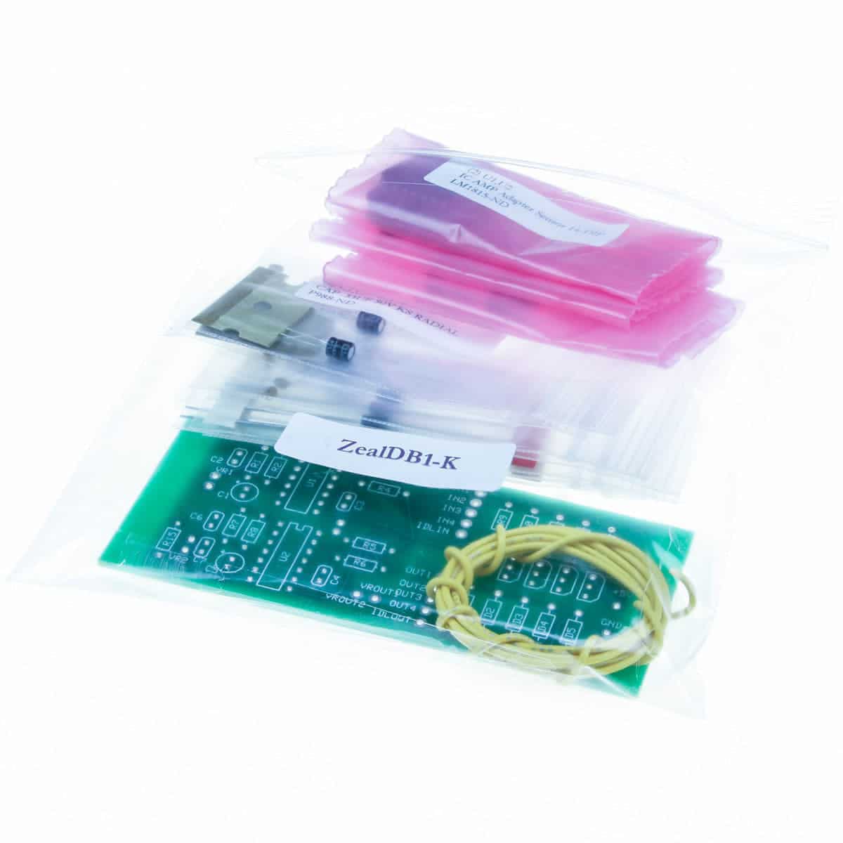
You can use this daughter card with any MegaSquirt version running MS1/Extra or MS2/Extra code. The card fits into the case lid. Here’s what circuits you get on the Zeal Engineering Daughterboard:
- 2 LM1815 VR conditioners optimized for the RX-7 and MS2/Extra
- 3 general purpose on/off outputs
- 1 12 volt tachometer driver
- 1 PWM IAC driver (max current 3 amps)
Bill of materials for the parts we include with this kit:
| Part number | Description | Quantity | Locations |
| P988-ND | 0.33UF capacitor | 2 | C1, C5 |
| BC1019CT-ND | 330pF capacitor | 2 | C2, C6 |
| 399-4149-ND | .01uF capacitor | 2 | C3, C4 |
| 399-2075-ND | .01uF capacitor | 1 | C7 |
| 1N4001DICT-ND | General purpose diode | 4 | D2-D5 |
| PN2222AD26ZCT-ND | NPN transistor (1A) | 4 | Q1-Q4 |
| ZTX688B-ND | NPN transistor (3A) | 1 | Q5 |
| 1.0MQBK-ND | 1.0M resistor | 2 | R1, R7 |
| 18KQBK-ND | 18K resistor | 2 | R2, R8 |
| 82KQBK-ND | 82K resistor | 2 | R3, R5 |
| 4.7KQBK-ND | 4.7K resistor | 2 | R4, R6 |
| 1.0KQBK-ND | 1.0K resistor | 5 | R9-R12, R14 |
| 470QBK-ND | 470R resistor | 1 | R13 |
| 330QBK-ND | 330R resistor | 1 | R15 |
| LM1815N-ND | Adaptive signal conditioner IC | 2 | U1. U2 |
Daughterboard Assembly
- Install all resistors in the indicated locations and solder into place.
- For RX-7s and most other applications, we have found that the second signal conditioner works better with the ground jumper installed in the two holes next to U2. Install a length of snipped resistor lead to bridge these holes, and solder into place.
- Install diodes D2 through D5, with the banded end towards the lower end of the card.
- Install C2, C3, C4, and C6.
- Install U1 and U2.
- Install C7.
- Install the Q1 through Q4 transistors, with the flat side on the transistor pointing to the flat side of the silk screen.
- Install Q5, again taking care to match its outline to the silk screen.
- Install C1 and C5. These capacitors are polarized; the long lead goes in the + hole and the white striped side goes in the other hole.
- Note that the VR connections (which you will hook up in the next steps) have the positive terminal next to the VR1 or VR2 marking, and the negative terminal furthest away from that marking.
There are a number of provisions for tuning the second VR conditioner on this board for other sensors besides the RX-7, though determining the best changes often requires an oscilloscope and some trial and error. If you are not getting good results with the default setup, options include substituting different values for C7 and R15, and not installing the jumper in step 2.
General Connections
Once you’ve got an assembled board, you can install it in the lid and connect it to the main board with lengths of wire. These connection points are used for all installations:
| Connection | V2.2 | V3.0 | V3.57 |
| +12V | Banded end of D9* | S12 | S12 |
| +5V | JP1 pin 8 | S5 | S5 |
| GND | Unbanded end of D2* | SG | SG |
| GND | Unbanded end of D3* | Proto GND | Proto GND |
* Normally, D2 and D3 are not installed in a V2.2 board. Use the holes on the empty slot. D9 is normally installed and would require soldering to the diode, although you will want to remove D9 if using the PWM IAC driver.
Using the VR Conditioners
On a V3.0 or V3.57 board, you can use the main board VR conditioner for the primary (NE) input, and the VR2 conditior for the secondary (G) input. On a V2.2 board, you’ll need both conditioners. You are best bringing both wires of the sensor all the way to the board, instead of grounding the negative wire. This reduces cross talk noise issues. You can bring the signals in on unused pins on the DB37 (or DB15, in the case of a V3.57 board) and use the appropriate jumper holes on the main board to connect to the conditioner. For example, if you brought the G sensor signal in on pin 25 for the positive terminal and 27 for the negative terminal on a V3.0/V3.57 board, you would connect the lower (positive) VR2 hole to IAC1A, and the upper (negative) hole to IAC1B. Here is where to connect VR2OUT to enable the second trigger.
| V2.2 | V3.0 | V3.57 | |
| MS1/Extra | U1 pin 11 | JS8 | JS8 |
| MS2/Extra | JP1 pin 5 | JS10 | JS10 |
If you wish to use the VR1 circuit, it’s a good idea to bring the negative VR wire in on an unused pin. For example, if you are wiring the VR sensor to pin 29, you would connect the negative (lower) VR1 terminal on the Zeal Engineering Daughterboard to IAC2A on a V3.0 or V3.57 board, or X13 on a V2.2 board. On a V2.2 board, remove D5, R10, D8, C12, U4, C11, and R11.
The upper (positive) VR1 terminal connects to different points depending on the board.
- V2.2 board: Unbanded end of D5
- V3.0 board: TachSelect
- V3.57 board: Pin 2 of JP1
Connect VROUT1 to the following pin:
- V2.2 board: Bottom end of R11
- V3.0 board; TSEL
- V3.57 board: Pin 2 of J1
JimStim testing
Testing the Zeal inputs on a JimStim can be tricky (and they won’t respond to a regular Stim at all). The LM1815 will not work with a square wave. You’ll want to use a 12 volt pull up on both the primary and secondary tach signal. For the primary tach signal, you can set the jumper for VR emulation. There is no correspoinding jumper for the secondary tach signal. Instead, put a 0.1 uF capacitor inline between the “2nd Trigger” connection on the JimStim and the VR input on the MegaSquirt. This will give a signal that can trigger the LM1815.
Using the PWM IAC driver
This can be used with V2.2 or V3.0 boards; we do not recommend it for V3.57 boards, which already can drive a PWM valve directly. The PWM driver can handle up to 3.0 amps, which works for many applications, although it is not as much current as a TIP120 can handle. It replaces the IAC circuit. On a V2.2 board, remove R16, Q5, and D9. On a V3.0 board, remove R19, Q4, Q20, R39, and D8. Connect the board using these points
| V2.2 | V3.0 | |
| IDLIN | Left end of R16 | Bottom end of R19 |
| IDLOUT | Lowest hole on Q5 | Banded end of D8 |
Tach Driver
The tachometer output can drive tachs that require a 12 volt signal. We’ve confirmed it works on first generation RX-7s, which would otherwise lose their tach signal if you dropped an FC ignition into one of them. Other tachometers may require different values of R14. The tach driver input is marked IN1, and the output is marked OUT1. The output can connect to any unused DB37 or DB15 pin, while we recommend the following pins as possible choices for input. Be sure you are not using them for other purposes.
MS1/Extra tach pins
| V2.2 | V3.0/V3.57 |
| X2 | JS0 |
| X3 | JS1 |
| X4 | JS2 |
| X5 | JS3 |
| U1 pin 15 | U1 pin 15 |
| U1 pin 10 | JS7 |
MS2/Extra tach pins
| V2.2 | V3.0/V3.57 |
| X2 | JS0 |
| X4 | JS2 |
| JP1 pin 4 | JS11 |
While MS2/Extra can also use LED circuits, FIDLE, or JS10 for tach outputs, we expect most Zeal Engineering Daughterboard installations will already be using these, so we recommend picking one of the above pins for tach control.
General Purpose Outputs
The Zeal Engineering Daughterboard has three general purpose on/off outputs, suitable for driving a relay or a solenoid with power consumption of 1 amp or less. The outputs are labeled OUT2, OUT3, and OUT4, while the inputs are labeled IN2, IN3, and IN4. The outputs connect to unused pins on the DB37 or DB15 connector. Here are the pins to use for inputs.
MS1/Extra spare outputs
| Output number | V2.2 | V3.0/V3.57 |
| 1 | X4 | JS2 |
| 2 | X5 | JS3 |
| 3 | U1 pin 15 | U1 pin 15 |
| 4 | U1 pin 8 | U1 pin 8 |
| Fan | X2 | JS0 |
MS2/Extra spare outputs
| V2.2 | V3.0/V3.57 |
| X2 | JS0 |
| X4 | JS2 |
| JP1 pin 4 | JS11 |
Just like with the tach driver, MS2/Extra can also use the LED circuits, JS10, or FIDLE as spare outputs, but they are not recommended as most are likely to already be taken by the ignition circuit or other purposes.